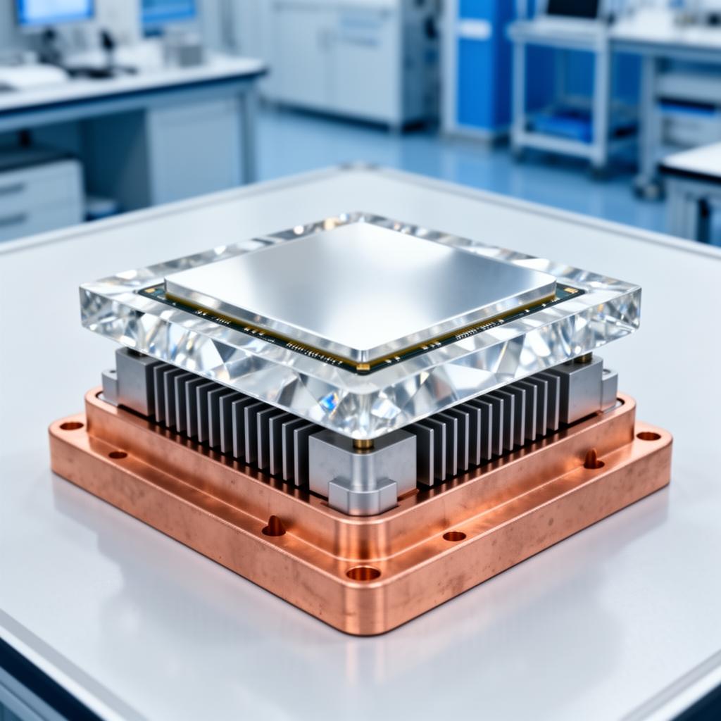
03CVD Diamond Application
Electronic Substrate
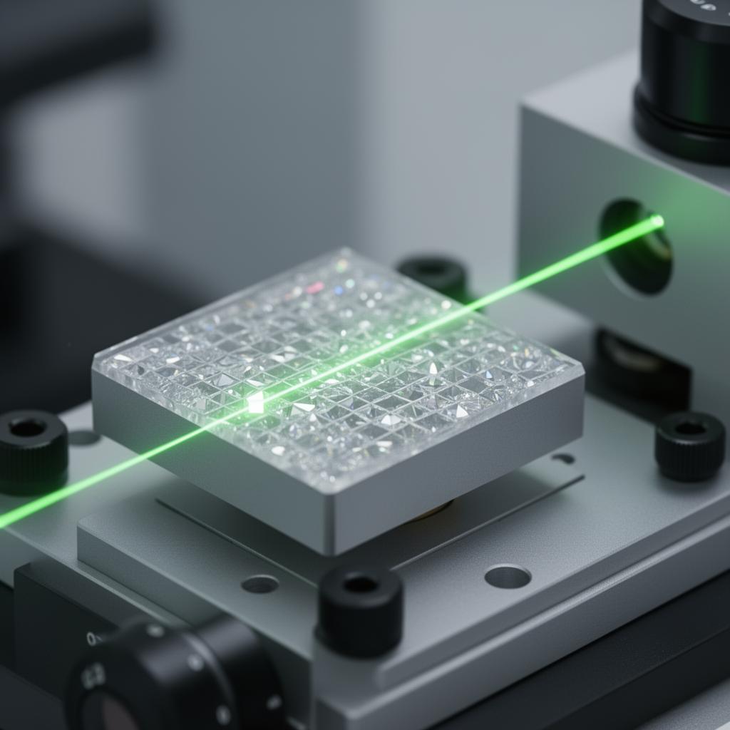
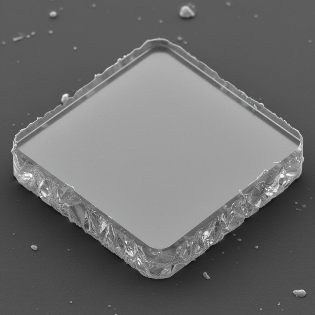
Monocrystalline Diamond — Electronic Grade
— Material
Mono CVD Diamond
— Specifications
- ◆Size: 3 – 10 mm+
- ◆Thickness: 0.04 – 4 mm
- ◆Orientation: (100) / (111) / (110)
- ◆Nitrogen level: 0.01 – 1 ppm
— Applications
- ◆MOSFET devices
- ◆High voltage semiconductors
- ◆UV detectors
- ◆RF electronics
- ◆Sensor devices
- ◆Advanced semiconductor R&D
— Key Features
- ◆Superior crystal quality
- ◆High carrier mobility potential
- ◆Excellent thermal dissipation
Need a custom electronic substrate solution?
Our engineering team supports laser cutting, double-side polishing, metallization, bonding and orientation cutting tailored to your process.
Talk to our team →— Other CVD Products